Welcome to Website of Prof. Saraju P. Mohanty
|
SRC
Grant P-10883: Fast PVT-Tolerant Physical Design of RF IC Components
Project Scope Background:
The uncontrollable statistical variability in device characteristics
represents major challenges to scaling and integration for present and
next generation nano-CMOS transistors and circuits. This in turn
demands revolutionary changes in the way in which current and future
integrated circuits and systems are designed. Strong links must be
established between circuit design, system design and fundamental
device technology to allow circuits and systems to accommodate this
increasing variability. Its major sources are: process variation (P),
supply voltage (V), and operating temperature (T) which may be due to
the environment, through self-heating effects or a combination of the
two. Unfortunately, process, voltage and temperature (PVT) variability
makes it hard to achieve “safe” integrated circuit designs in nanoscale
technology and also causes loss of yield. While some attempts have been
made to address PVT variation issues in digital circuits, no attempts
have been made to address these for mixed-signal, analog, and radio
frequency (RF) integrated circuits (IC) due to the increased complexity
of the designs. Thus, the research will immensely advance the
state-of-the-art of RF-IC design methodology. Description:
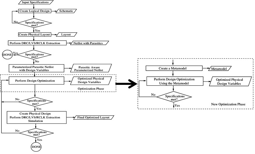
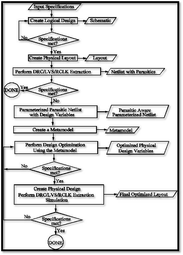
To have a process-variation robust design accounting for parasitics,
power, and temperature, we will investigate a new “PVT tolerant RF IC
design flow”. In a standard RF IC design flow, multiple iterations
between the front-end circuit design and back-end layout are required
to achieve parasitic closure. Such a manual approach requires X number
of iterations. The goal of the proposed design flow is to reduce the
number of manual iterations to 1, by performing the X number of
iterations on a parasitic parameterized netlist instead of the layout.
The parasitic parameterized netlist refers to the netlist derived from
the initial physical design and then parameterized for optimization in
X automatic iterations. The final physical design is done using the
parameters obtained from the netlist optimized for a worst case process
variation. This constitutes 1 iteration. Hence, this novel flow reduces
the X number of manual iterations required for parasitic closure, to 1
manual iteration. This flow ensures that the final physical design is
not only resistant to parasitic effects, but also process-variation
tolerant. Thus, the RF IC design cycle can be significantly reduced
resulting in lost cost RF ICs while enhancing PVT tolerance of the RF
ICs, which will improve the RF IC yield. We will analyze average and
worst case variations for standard nano-CMOS RF IC components such as
VCOs and LNAs including: (1) center frequency, (2) phase-noise, (3)
linearity, (4) throughput, (5) dynamic power dissipation, (6)
subthreshold leakage, and (7) gate-oxide leakage. We will then
investigate the use of conjugate gradient method, simulated annealing
method, and Monte Carlo method for optimization of various physical
parameters once the parameterized full-blown parasitic netlist of an RF
IC is obtained. We recently performed conjugate gradient method based
optimization of center frequency of a nano-CMOS VCO. Primary Anticipated
Result:
Novel design and optimization methodologies (not design) that can
produce PVT-tolerant RFICs in one design iteration only and with
minimal (at most two) manual layout steps to improve circuit yield (by
accounting for process variation effects right at the design stage) and
reduce chip cost. Project Personnel Faculty:
Students:
The
contributions include -- Implementing the ideas, generating the
results, compiling results for publication, and making conference
presentations.
Project Publications
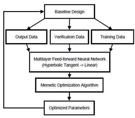
Project Deliverables Nonpolynomial Metamodeling Based Mixed-Signal Optimization using Memetic Algorithm: Refer the following presentation for details: Mohanty_ISQED2012-Memetic_Talk.pdf Fast mixed-signal design optimization flow that combines nonpolynomial metamodels and memetic optimization algorithm.
Feed-forward dual layer (FFDL) neural newtorks are considered for nonpolynomial metamodeling. FFDL neural-networks are created for each figure-of-merit (FoM) of the phase-locked loop (PLL) components in which non-linear hidden layer functions are considered each with varying hidden neurons of 1 to 20. Memetic algorithm is considered for optimization over the neural-network metamodels.
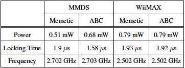
A 180nm phase-locked loop (PLL) is considered as a case study circuit. A total of 21 parameters for transistor sizing are considered during optimization. Two different specifications of PLL design completed using once created metamodels to demonstrate the reusability of the metamodels.
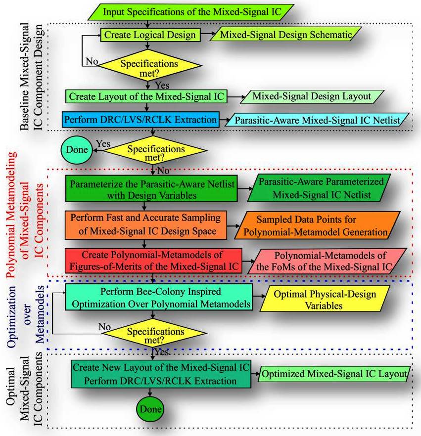
Polynomial Metamodeling Based Mixed-Signal Optimization using Bee-Colony Algorithm: Refer the following presentation for details: MohantyISED2011Talk_PLL-BC-Optimization.pdf Fast mixed-signal design optimization flow that combines polynomial metamodels and artificial bee colony (ABC) optimization algorithm.
A 180nm phase-locked loop (PLL) which is the heart of all synchronous circuits and systems is used as a case study circuit.
Polyonomial metamodels of the figures-of-merits (FoMs) of the PLL components are used in the design flow.
Artificial bee colony algorithm is used for the optimization over polynomial metamodels. In the algorithm, position of a food source --> a solution; Nectar amount --> Quality of a solution; Number of worker bees --> number of solutions in the population.
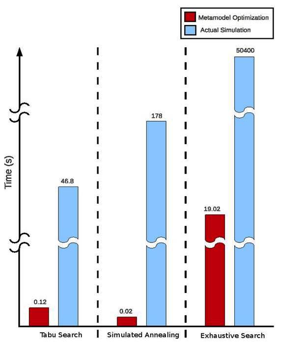
Polynomial Metamodeling Based Mixed-Signal Design Optimization: The fast and yet accurate single-iteration design flow that combines polynomial metamodels and selected optimization algorithms.
Three Optimization Algorithms: Exhaustive, Tabu-Search and Simulated-Annealing invesitgated,
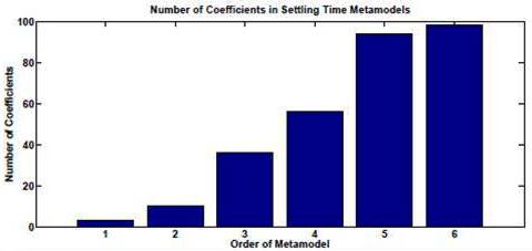
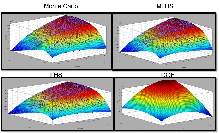
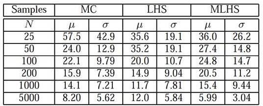
Sampling Techniques for Accurate Metamodeling: Refer the following presentation for details: MohantyISED2010MetamodelingTalk.pdf The fast and yet accurate single-iteration design flow that combined metamodels and optimization algorithms.
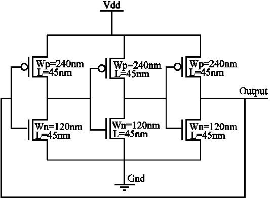
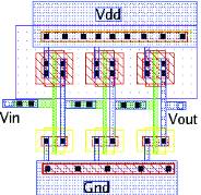
Design of 45nm Ring Oscillator Circuit.
The sampling techniques applied to the 45nm Ring Oscillator Circuit.
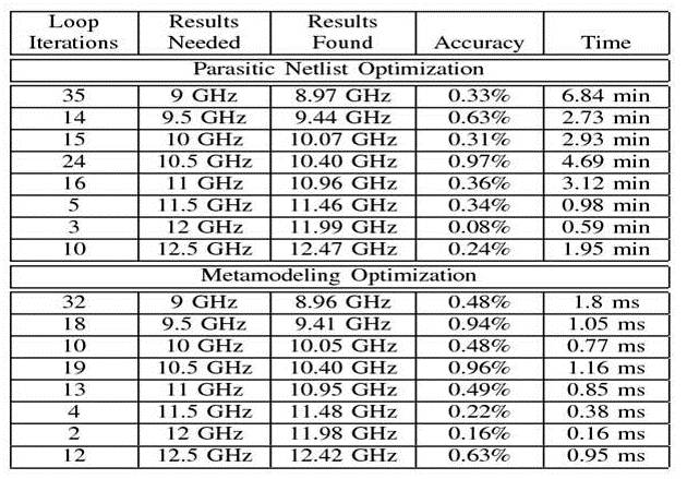
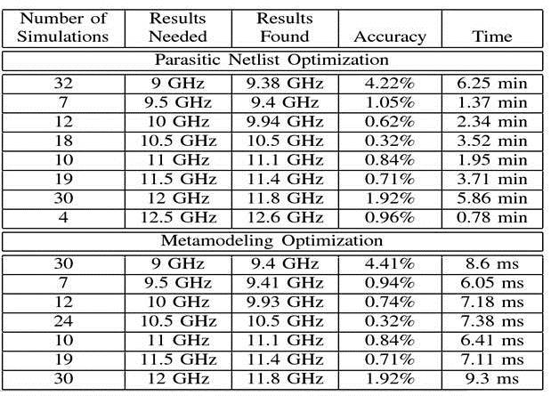
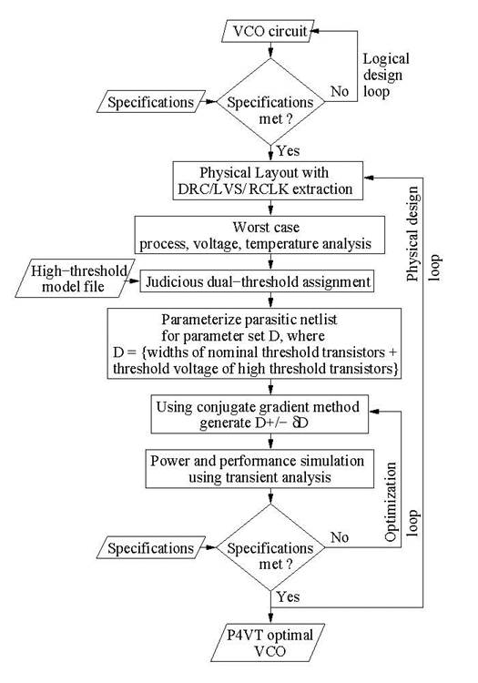
Accurate and Single Iteration Design Flow: Refer the following presentation for details: MohantyICVD2010P4VTtalk.pdf The accurate design flow for P4VT optimal VCO. This achieves design closure in one manual iteration involving two manual layouts only.
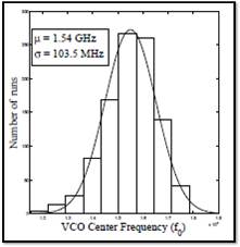
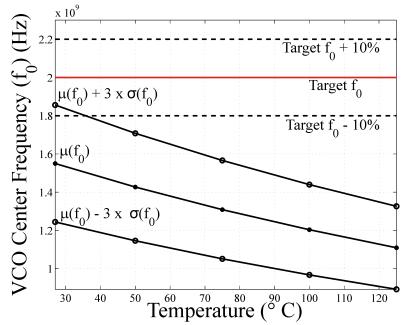
PVT Variation Analysis of VCO for different FoMs.
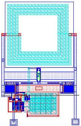
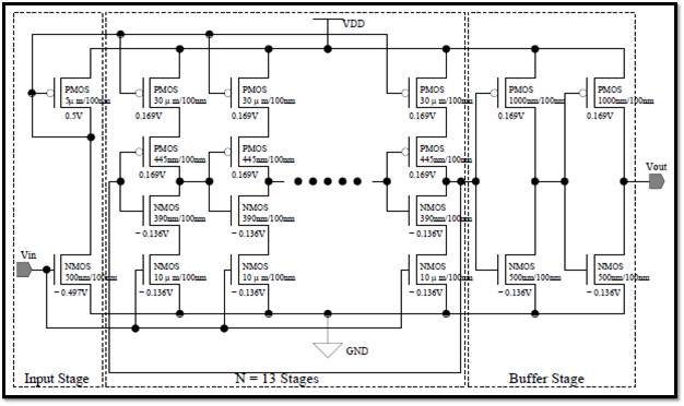
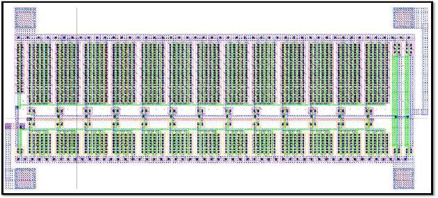
The P4VT optimal VCO Design.
|
Home |
 |
 |
 |
Last
updated on 01 Jan 2013 (Tuesday).
©
Saraju P. Mohanty


